PACKAGING / OPTOCPO WHITE PAPER
Why Optical I/O Coupling Fails at the Package Level
A practical guide to coupling loss, alignment tolerance, and package yield for CPO and silicon photonics teams.
Abstract. A fiber-to-chip coupler does not fail on a perfect simulation plot. It fails when the fiber block shifts, the adhesive cures, the package heats up, and the worst channel in the array loses margin. Device efficiency matters, but the product decision is whether every required channel can pass after assembly. This paper shows where teams miss that risk and what to model and measure before the design is locked. The numerical comparison is illustrative, not measured OptoCPO data.
Who should read this? Teams choosing among edge, grating, lens-assisted, interposer, or optical-bridge interfaces; teams whose measured package loss differs from simulation; CPO, NPO, silicon photonics, optical I/O, and dense fiber-array teams; and anyone preparing a supplier review, investor review, or architecture decision.
1. Peak coupling efficiency is not enough
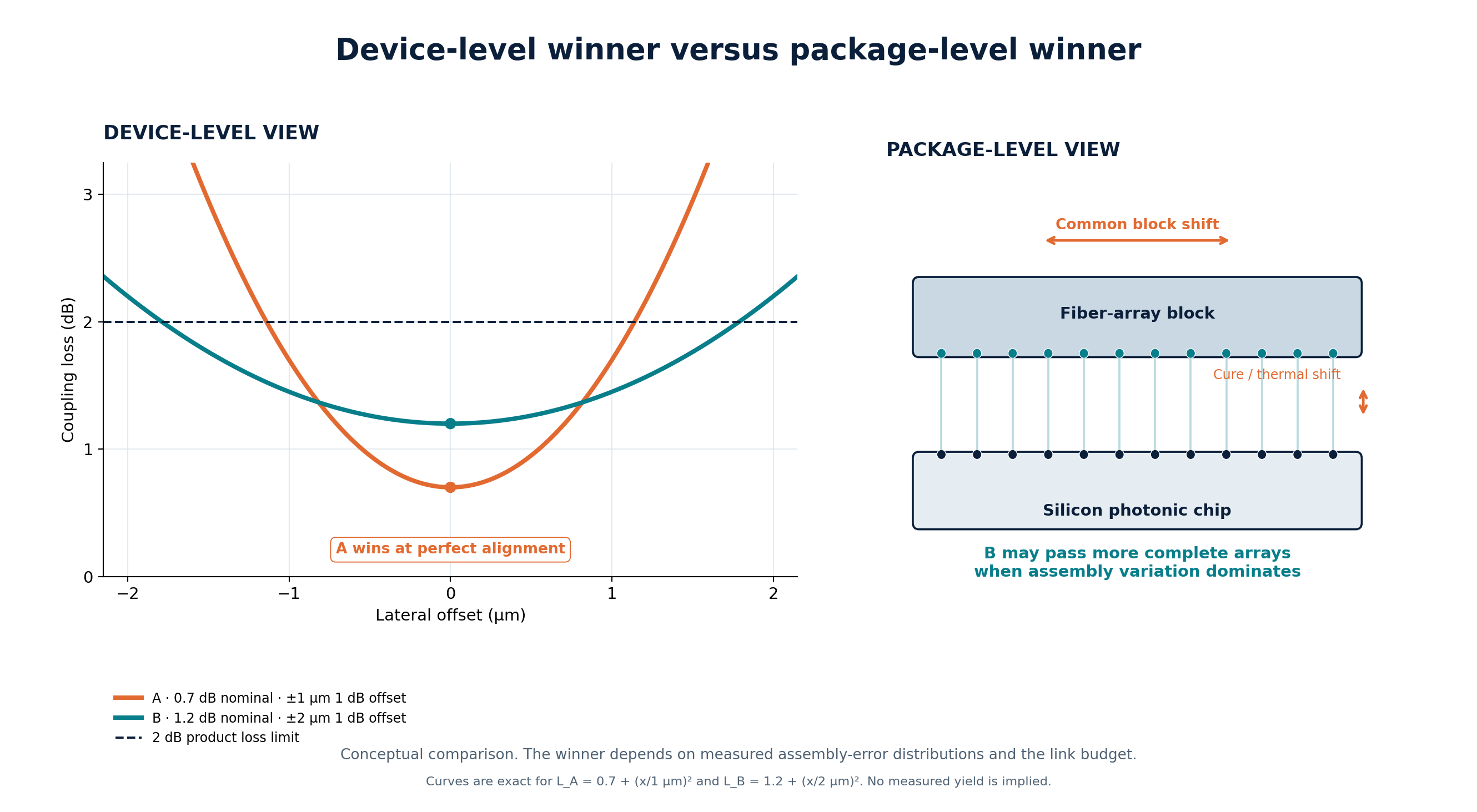
Two hypothetical fiber-to-chip couplers are on the table. Candidate A has 0.7 dB nominal loss and gains another 1 dB at ±1 µm lateral offset. Candidate B starts at 1.2 dB but does not gain another 1 dB until ±2 µm. On a perfectly aligned device plot, A wins by 0.5 dB. On a production line, the answer depends on where the fibers actually land and how far they move after bonding.
The example is illustrative. It is not a measured comparison of edge and grating couplers, and neither architecture is assigned to A or B. If the attach process holds position tightly and the link budget cannot accept 1.2 dB, A may be right. If placement and cure shifts are larger, B may give more passing packages. To decide, set a port loss limit and use measured assembly errors to test the whole array.
In production, the winning design is not the lowest-loss port; it is the lowest-risk passing package.
Figure 1 shows the decision plainly: A has lower loss at perfect alignment but a tighter lateral window; B starts with higher loss but tolerates more displacement. A wins the device-level comparison, while B may be the better package-level choice when assembly variation dominates.
A fiber array moves as a block. Lateral and vertical shifts, roll, tilt, and pitch error can put the center channel near its optimum while the outer channels lose margin. The adhesive can pull the array during cure. Temperature changes the gap or relative position of the fiber block and die. Mechanical stress can alter geometry or optical properties. A coupler must also work over the specified wavelengths and polarization states without unacceptable return loss. Fiber routing and strain relief may restrict where the block can sit.
A late surprise is expensive. If the selected coupler needs a tighter process than the assembler can sustain, the team may add active-alignment time, rework bonded units, scrap packages, demand more laser power, or redesign the PIC and fiber assembly. The cost to track is cost per passing channel in a qualified package, including attach, test, rework, and yield. A best-port number does not estimate it. Dense CPO interfaces must meet yield and scale requirements alongside optical specifications, as imec notes.
2. Five mistakes that create optical I/O risk
Table 1. Common mistakes and their business consequences
| Mistake | What goes wrong technically | What it costs | Better practice |
|---|---|---|---|
| 1. Report only peak simulated loss | A single optimum hides a steep loss surface and weak edge ports | Wrong architecture chosen before attach capability is known | Show loss maps and worst-port results over defined conditions |
| 2. Ignore alignment tolerance | x, y, gap, angle, pitch, or roll takes channels out of budget | More active-alignment time, lower yield, rework | Report 1 dB and 3 dB windows and test the joint array error |
| 3. Simulate the coupler without the package | Lens, adhesive, gap, lid, substrate, and block change fields or position | Late package workaround or new die revision | Model the assembled stack; measure before and after cure |
| 4. Ignore wavelength, polarization, or return loss | A WDM channel, input state, or laser-feedback limit fails | Lost margin, more laser power, added isolation | Check the complete optical and thermal operating envelope |
| 5. Equate wafer test with the product port | Test gratings and production ports have different paths and planes | Misstated production loss and yield | De-embed test ports; measure the shipped interface |
A peak number needs a reference plane. “0.7 dB coupling loss” could mean one fiber-to-PIC transition or a value extracted from fiber-to-fiber transmission through two couplers and a waveguide. It may be measured at the optimum position or after a permanent bond. Ask what is included, how propagation loss was removed, and what happens at the worst specified condition. Otherwise, apparently comparable data can support the wrong decision.
An alignment window is not an assembly yield. A ±1 µm lateral 1 dB tolerance says little about vertical error, fiber angle, or accumulated pitch error. One common block shift can affect every port; roll may punish the outer ports most. The 3 dB window can help an active-alignment system capture light, but the product may allow far less than 3 dB additional loss. Measure what the process holds after cure, not just what it can find before bonding.
The package changes the optical problem. A lens can improve field matching while introducing tilt sensitivity and another reflecting surface. An adhesive's index and bondline affect the field and working distance; its shrinkage moves the optic. A lid and fiber strain relief can constrain a theoretically ideal position. Modeling the coupler alone is appropriate for screening geometry, but insufficient for approving the optical interface.
Operating conditions expose hidden failures. A surface grating can shift response with wavelength and process variation. A polarization-sensitive transition may fail when the incoming state changes. Reflected light may disturb an external laser even though forward loss passes. Evaluate the data path and the laser-feed path separately across their actual conditions.
A wafer probe is a learning interface. Grating test ports can accelerate characterization, but a final package may use edge coupling, a bonded grating array, or an interposer. De-embed the probe path, then validate the production transition. A wafer result should not silently become a package loss specification.
3. From coupling loss to coupling confidence
Use this workflow before freezing the architecture. Record what each model assumes and what measurement will challenge it.
1 — Draw the optical path and name the reference planes. Separate the laser feed, modulated data path, and test path. Mark the fiber-to-chip, chip-to-chip, interposer, connector, and waveguide interfaces that actually exist. Allocate insertion-loss and reflection limits to each. This prevents a pair-of-couplers result from being treated as a one-interface result and identifies the path that is short of margin.
2 — Build the device-level optical model. Calculate the fiber and waveguide modes and their power-normalized overlap. Use EME for a long guided taper, full-wave electromagnetic modeling for finite gratings or scattering regions, and RCWA to screen periodic grating choices. Check material dispersion, mesh convergence, boundary conditions, polarization, and reflected power. Deliver a field or scattering response across the required operating range, not just a peak efficiency.
3 — Add package optics. Place the simulated interface into the real fiber array, lens or lenslet, adhesive, air gap, glass block, lid, and interposer stack as applicable. Use physical-optics propagation when diffraction and phase matter; use ray tracing to assess larger lens paths, clearances, and stray paths. Include the actual mechanical access for alignment and fiber routing. The output should be loss and reflection versus package position, not another ideal-device value.
4 — Add thermal and mechanical movement. Estimate die shift, substrate bow, expansion mismatch, adhesive cure movement, bondline changes, and stress at assembly and operating temperatures. Feed displaced geometries back into the optical calculation. Compare pre-bond optimum, post-cure state, and hot/cold states. If those positions differ, the alignment setpoint may need to anticipate movement.
5 — Calculate full-array tolerance and yield. Sweep lateral, vertical, gap, angular, pitch, and relevant fabrication variation. Use measured process distributions where available. Sample one block translation and rotation per virtual assembly; sample independent local port errors separately where justified. Count a package as passing only when all required channels meet their limits. With limited process data, report a sensitivity analysis rather than a confident yield prediction.
6 — Close the loop with measurement. Perform alignment scans and record their shape, not only the best point. Measure spectra, polarization-dependent loss, return loss, near or far field where useful, and each channel's response before and after cure and thermal exposure. Use reference structures to separate waveguide propagation from coupling. If the measured loss map disagrees with simulation, revisit the field, geometry, materials, and reference planes before declaring the model validated.
The loop does not end when one measured loss number agrees with simulation. Use the measured loss maps to update the fields, as-built geometry, material assumptions, and shared and local error distributions; then check whether the revised model predicts independent packages. That measurement correlation is what turns a plausible model into a useful design tool.
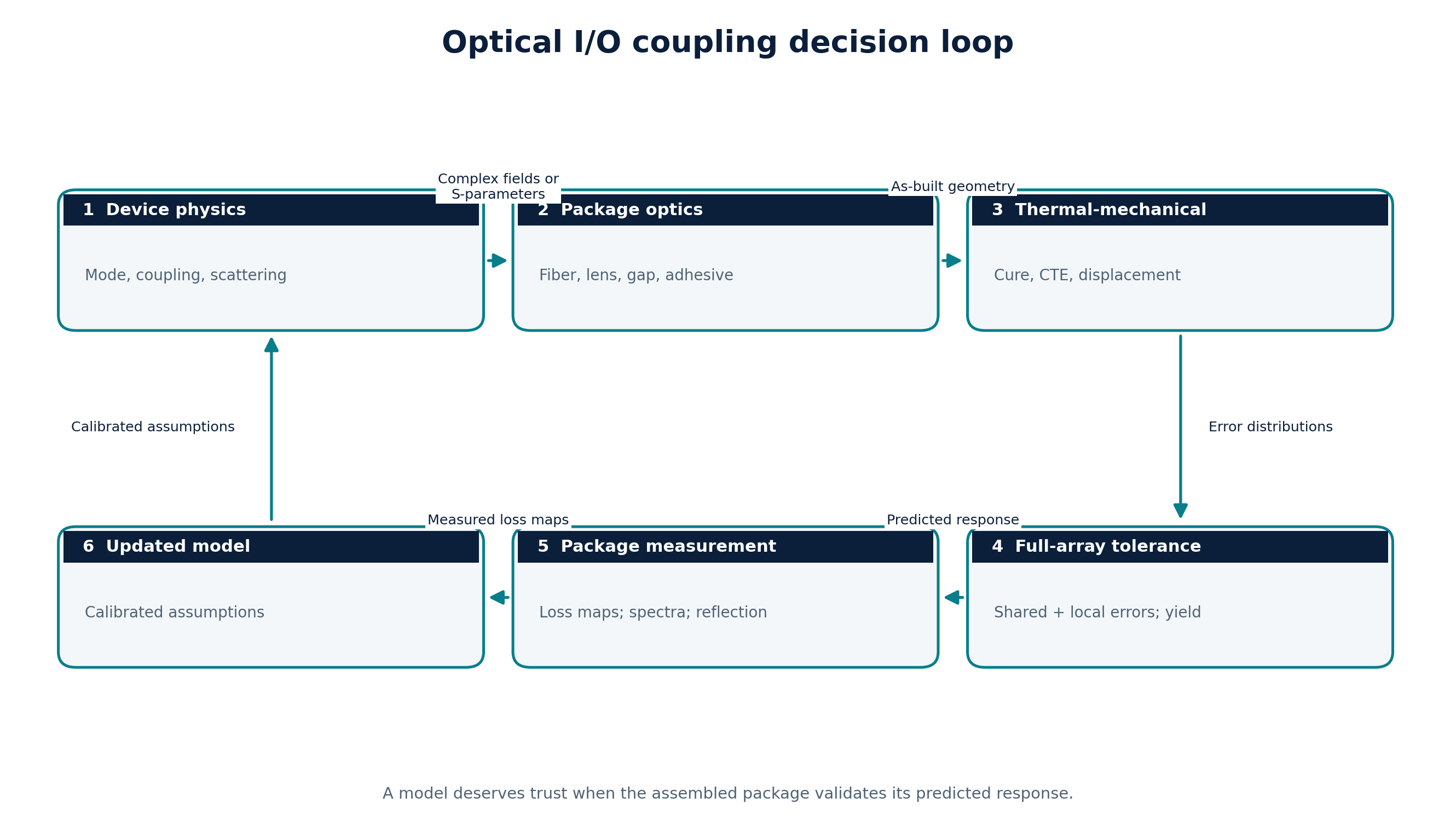
No single software suite owns the full decision. Teams may combine electromagnetic solvers, physical-optics or ray-tracing tools, thermal-mechanical analysis, circuit/link modeling, and Python-based tolerance or Monte Carlo workflows. The value is in the handoff between fields, reference planes, geometry, material data, error distributions, and measurement. Depending on the problem, examples include Lumerical, Zemax OpticStudio, COMSOL, Synopsys/RSoft, Tidy3D, Meep, JCMsuite, Photon Design, IPKISS, gdsfactory, KLayout, and Python.
4. OptoCPO perspective: coupling is a system-level decision
OptoCPO’s position is that optical I/O coupling is a system-level design decision. Electromagnetic simulation shows what the interface can do. Package optics show where that performance survives. Thermal-mechanical and tolerance analysis show how often. Measurement shows whether the model deserves trust.
Ask instead: Which interface can meet the link budget, survive the package, pass across all required channels, and scale to manufacturing? An edge taper, surface grating, lens-assisted interface, or optical bridge may answer it in different ways. The choice depends on the foundry stack, fiber access, wavelength range, attach process, laser constraints, and service plan. No peak-efficiency ranking replaces those inputs.
Before a design review, bring three items: an optical-path drawing with reference planes; loss and reflection maps that include the worst channel and operating corners; and a test plan that can separate a device error from an assembly error. If one is missing, a targeted coupon or alignment scan may be more valuable than another round of nominal geometry optimization.
OptoCPO Coupling Risk Checklist
- Are input and output reference planes defined for each loss result?
- Are laser-feed, data, and wafer-test paths shown separately?
- Is loss reported over required wavelength and polarization conditions?
- Are 1 dB and 3 dB alignment windows known in relevant axes?
- Are the fiber block, adhesive, gap, lens, lid, and stack included where relevant?
- Are common array errors separated from local port errors?
- Is return loss included in the laser and link analysis?
- Is drift assessed after bonding and over temperature?
- Is the wafer test port separated from the shipped interface?
- Does the decision use package yield and cost per passing channel?
Each “no” points to a task before a team can claim manufacturing readiness. Optical, packaging, test, and product owners should answer together.
Method note. The 0.7 dB versus 1.2 dB comparison is conceptual. It is not measured OptoCPO data or a production-yield forecast. Replace its assumed tolerance behavior with process-specific simulation and assembly measurements before selecting an architecture.
Teams can share an architecture boundary or technical constraint that may inform a future OptoCPO educational note.
Share a coupling question ↗